Designing a 4S Smart BMS with the BQ76920: Every Trap I Hit and How I Fixed It
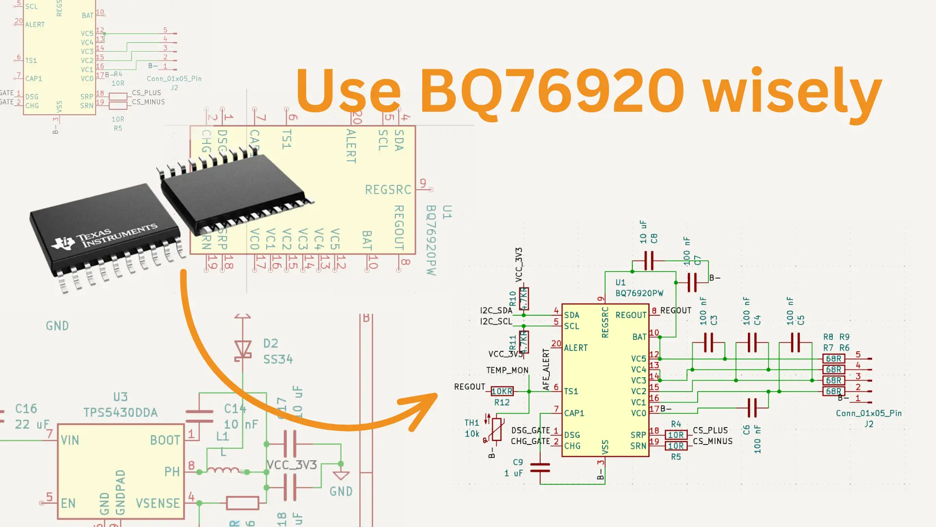
Most BMS tutorials show you a finished board. This one is about the schematic stage — specifically, every mistake I caught and fixed before sending a board to fabrication, where they would have cost real money and weeks of time.
I am building a modular Smart BMS for a 4S Lithium-Ion pack, designed to pair with an ESP32-S3 for I2C-driven state monitoring and eventual AI-predictive cell health estimation. The Analog Front End is Texas Instruments’ BQ76920 — a well-documented chip that still hides several non-obvious traps for anyone who reads the datasheet too quickly. The power supply is a TPS5430DDA buck converter regulated to 3.3V.
What follows is a complete audit of every schematic error I caught and corrected, with the KiCad screenshots as proof. If you are designing around either of these chips, this post will save you at least one board spin.
The Hardware at a Glance
- AFE: Texas Instruments BQ76920 (natively 5S, configured for 4S)
- MCU: ESP32-S3 (I2C master, ALERT monitoring, gate command via BQ76920)
- Power Supply: TPS5430DDA non-synchronous buck converter → 3.3V rail
- Cell configuration: 4S Lithium-Ion, balancing via BQ76920 internal FETs
- Toolchain: KiCad 8.0
Part 1 — The BQ76920 AFE: Analog Safety Core
The 4S Cell Mapping Trap
This is the trap that will destroy your board silently if you miss it.
The BQ76920 is natively a 5-cell (5S) chip. It has six cell voltage sense pins: VC0 through VC5. For a 4S pack you only have four cells, which means one of these pins must be handled correctly — and “correctly” is not what your intuition suggests.
The two wrong approaches people try:
- Leave VC4 floating — the internal reference circuit sees an indeterminate voltage on an active sense pin. The chip’s overvoltage protection trips immediately or the cell balancing FET for that channel turns on into nothing and heats up.
- Short VC4 to VC5 — same problem. You are telling the chip cells 4 and 5 are at identical voltage, but cell 4’s balancing path is still live.
The correct approach, per TI’s application note, is to short VC3 and VC4 together and connect both to Cell 3 Positive. This collapses the phantom 5th cell out of the measurement chain entirely. The chip sees zero differential voltage across that cell slot, the balancing FET for that slot stays off, and the remaining four cells map correctly.
The exact pin mapping for 4S:
| BQ76920 Pin | Connection |
|---|---|
| VC0 | B− (pack negative) |
| VC1 | Cell 1 positive |
| VC2 | Cell 2 positive |
| VC3 | Cell 3 positive |
| VC4 | Cell 3 positive (shorted to VC3) |
| VC5 | Cell 4 positive |
| BAT | Cell 4 positive |
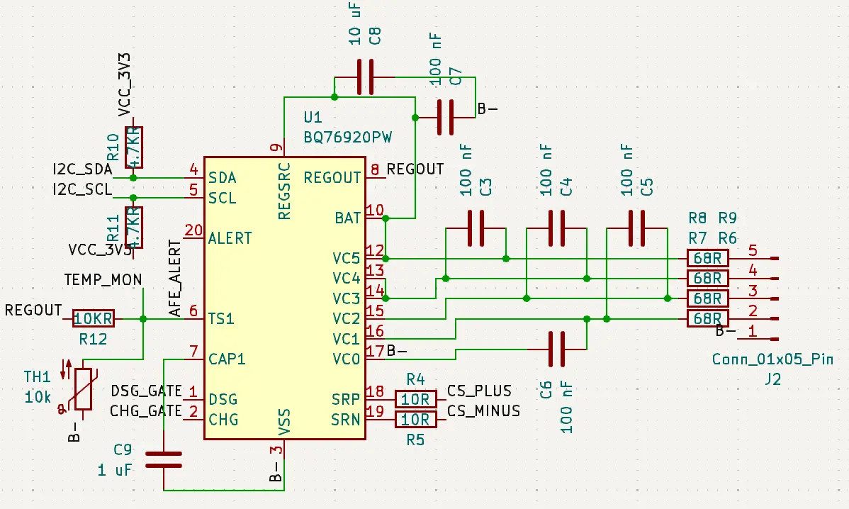
BQ76920 with correct 4S pin mapping. VC3 and VC4 are shorted and tied to Cell 3 positive. Each cell tap line has a 68Ω series resistor and 100 nF filter cap to ground.
Missing Balancing Resistors
The BQ76920 has internal cell balancing FETs that dump charge from higher cells through an external resistor path during top-balancing. I had placed the 100 nF filter capacitors on every cell tap line — but completely missed the 68Ω series resistors that must sit between each VCx pin and the cell tap node.
Without these resistors, the balancing FET sees the full cell capacitance directly. When the FET switches, the inrush current through the trace is not limited. At anything above a few milliamps, this will eventually damage the internal FET or cause measurement errors on the ADC during a balance cycle.
The 68Ω resistors combined with the 100 nF caps also form a low-pass RC filter (corner frequency ≈ 23 kHz) that attenuates switching noise from adjacent cells into the voltage sense lines. Without them, the ADC reads noise-contaminated cell voltages and the SoC estimation drifts.
Fix: four 68Ω resistors added in series on VC1 through VC4 tap lines, between the cell node and the VCx pin.
Capacitor Ladder Placement Error
The 100 nF decoupling capacitors on the cell tap lines must form a ladder to the negative rail — each capacitor bridging the gap between adjacent VCx lines (C between VC0–VC1, VC1–VC2, VC2–VC3, VC3–VC4, VC4–VC5). In my first pass, C3 was placed in parallel with C5 instead of bridging its correct VC1–VC2 gap. Two capacitors decoupled the same node pair, leaving the VC2–VC3 gap completely unfiltered.
This is the kind of error that passes DRC silently — no short, no missing connection, no ERC flag. The only way to catch it is to trace each cap placement by hand against the TI reference schematic.
The REGOUT Typo on the Thermistor Circuit
The BQ76920 has a REGOUT pin that provides a regulated reference voltage, intended to power external components like the thermistor circuit for temperature monitoring. In my schematic I had accidentally placed a net label reading “EGOUT” on the thermistor bias resistor instead of a physical wire connection.
Net labels in KiCad create a logical connection — so “EGOUT” was a floating net that connected to nothing. The ERC caught this as an unconnected net, but only because no other label in the schematic matched the typo. In a larger schematic with more nets, a one-character typo in a label name can silently create a disconnected net that passes ERC if the label appears elsewhere.
Fix: deleted the label entirely, drew the wire directly from the REGOUT pin to the thermistor bias resistor R12.
Part 2 — The TPS5430DDA Buck Converter: 3.3V Power Rail
The TPS5430 is a 3A synchronous buck converter. Straightforward to design with — once you know where the datasheet traps are.
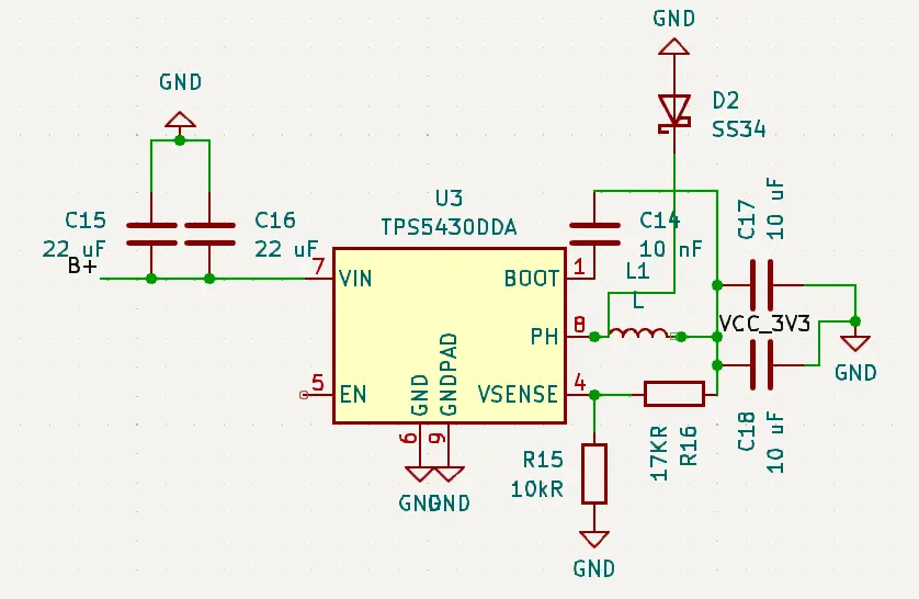
TPS5430DDA configured for 3.3V output. Bootstrap cap C14 is 10 nF. Schottky SS34 on PH pin. Feedback divider R15 (10kΩ) and R16 (17kΩ) sets VSENSE for 3.3V output.
The Fatal Feedback Resistor Math Error
This is the one that would have fried the ESP32-S3.
The TPS5430 sets its output voltage through a resistive divider from VOUT to VSENSE to GND. The internal reference voltage is 1.221V (datasheet Section 7.3). The formula is:
VOUT = 1.221V × (1 + R_top / R_bottom)
With R_bottom fixed at 10 kΩ (R15), solving for 3.3V output using the correct TPS5430 reference of 1.221V (datasheet Section 7.3):
3.3 = 1.221 × (1 + R_top / 10000)
3.3 / 1.221 = 1 + R_top / 10000
2.7026 - 1 = R_top / 10000
R_top = 17,026 Ω  →  17 kΩ standard E24 value ✓
Verification:
VOUT = 1.221 × (1 + 17000 / 10000) = 1.221 × 2.7 = 3.297V ✓
The AI-generated design document I was working from stated the formula with a reference voltage of 0.891V — a value that does not appear anywhere in the TPS5430 datasheet. Using that wrong reference, the document calculated R_top = 27.4 kΩ. That value sounds reasonable in isolation. It is not. Plugging 27.4 kΩ back in against the actual 1.221V reference:
VOUT = 1.221 × (1 + 27400 / 10000) = 1.221 × 3.74 = 4.567V ← destroys ESP32-S3
The ESP32-S3 absolute maximum on VDD is 3.6V. A 4.56V rail applies power the moment you connect the battery. There is no soft start that saves you. The module is dead before firmware runs a single instruction.
The fix is R16 = 17 kΩ, which is exactly what the schematic shows. The document was wrong. The schematic is correct.
The Missing Catch Diode
The TPS5430 is a non-synchronous buck converter — its PH (switch) pin swings between VIN and GND as the internal high-side FET switches. When the FET turns off, the inductor current must continue flowing. Without a freewheeling path, the inductor forces the PH node below GND, potentially to −40V on a fast-switching edge, which exceeds the TPS5430’s PH pin rating and destroys the chip.
The required component is a Schottky diode from PH to GND — cathode at PH, anode at GND. The Schottky’s low forward voltage (≈0.3–0.4V) clamps the PH node just below GND and provides the freewheeling path for inductor current during the off-time.
I had the inductor, the bootstrap cap, and the output filter, but the Schottky was missing entirely from the first revision. This would have caused immediate oscillation or chip failure on first power-up.
Fix: SS34 Schottky diode added from PH to GND. The SS34 is rated for 3A forward current and 40V reverse voltage — matching the TPS5430’s 3A output and well above the VIN maximum.
The Bootstrap Capacitor Typo
The BOOT pin on the TPS5430 requires a 10 nF bootstrap capacitor (C14 in the schematic) between BOOT and PH. The bootstrap cap charges when PH is low and provides the gate drive voltage for the internal high-side FET when PH swings high — a standard bootstrap topology.
My schematic label read 10 µF — three orders of magnitude wrong. A 10 µF capacitor on BOOT would not charge and discharge fast enough to supply the gate drive at the switching frequency, degrading the gate drive voltage and causing shoot-through losses. The TPS5430 datasheet is explicit: 10 nF, ceramic, X5R or better.
Part 3 — ESP32-S3 Gate Control: What Not to Wire
The original AI design document instructed me to wire two ESP32-S3 GPIO pins directly to the DSG (discharge) and CHG (charge) MOSFET gate pins of the BQ76920 to “manually control” the gates from firmware.
This is architecturally incorrect and was removed from the final schematic.
The BQ76920’s DSG and CHG pins are outputs from the AFE, not inputs. They are gate drive lines controlled internally by the BQ76920’s protection logic and by I2C register commands (specifically the SYS_CTRL2 register, bits CHG_ON and DSG_ON). The correct firmware flow is:
- ESP32-S3 sends I2C write to BQ76920
SYS_CTRL2register - BQ76920 toggles DSG or CHG gate drive internally
- External MOSFETs switch
Driving those gate pins from a GPIO simultaneously would create a bus conflict — the ESP32’s GPIO and the BQ76920’s internal gate driver would fight each other. In the worst case, the output stage of one or both devices is damaged. At minimum, the protection logic breaks.
Boot Circuit
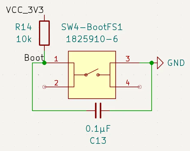
Boot switch circuit. R14 (10 kΩ) pulls Boot high to VCC_3V3. SW4 (1825910-6) momentary SPST pulls the line low when pressed. C13 (0.1 µF) debounces the switch. Pin 3 of the connector goes to GND to complete the circuit.
The boot switch circuit is straightforward: a 10 kΩ pull-up to VCC_3V3 keeps the ESP32-S3 BOOT pin high (normal operation). Pressing SW4 pulls the pin low, which puts the chip into download mode on the next reset. C13 at 0.1 µF handles mechanical bounce on the switch contacts. Nothing unusual here — documented for completeness.
What’s Next
This schematic is complete and will go into layout once I finalize the MOSFET selection for the DSG and CHG paths (targeting 30V, 10A rating with low RDS(on) for the expected discharge currents). The board will be a two-layer design fabricated via JLCPCB.
The next post on this project will cover the PCB layout decisions: copper pours for the high-current discharge path, thermal relief on the MOSFET pads, and the placement strategy for keeping analog cell-sense traces away from the switching node of the buck converter — a real interference problem on a mixed-signal board this small.
The firmware side — I2C initialization, register map for the BQ76920, and the ESP32-S3 state machine for charge/discharge management — will follow once the board is in hand and validated.
Every error documented here was caught at the schematic stage. The cost of catching a wrong resistor value in KiCad is five seconds and a backspace key. The cost of catching it after fabrication is a new board order, two weeks of shipping, and a potentially destroyed ESP32. Audit your math. Trace every net. Read the datasheet figures, not just the text.